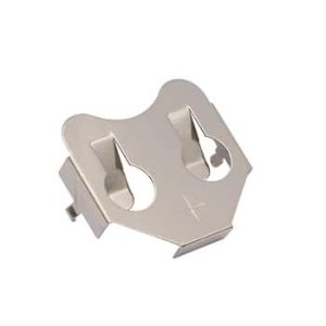
Engineering Datasheet: THM Battery Contact, Direct Footprint Replacement for Keystone 52
Securing power continuity for cylindrical cells on high-density FR4 boards demands absolute pin coplanarity to withstand wave soldering turbulence. The Jiatel JT-BC-AA-KS52 functions as a high-reliability, 1:1 direct footprint replacement for the industry-standard Keystone 52 contact. Engineered specifically with a dual-pin THM architecture, it allows hardware engineers to execute seamless board-level power integration without altering existing PCB drill hole layouts or solder pallet designs.
Verified Board-Level Parameters
| Target Cross-Reference | Direct Footprint Replacement for Keystone 52 |
| Mounting Architecture | Through-Hole Mount (THM) Dual Pin |
| PCB Pad Pitch | 7.62mm Contact Pin Spread (Ø1.90mm Drills) |
| Axial Layout (“L” Dim) | 33.00mm (AA) | 16.50mm (CR123A) | 9.40mm (CR2) |
| Base Metallurgy | T=0.30mm Spring Steel | Nickel Plated |
Target Deployments
- Industrial IoT: THM sensor nodes utilizing CR123A/CR2 lithium cells.
- Medical Diagnostics: Compact patient monitoring PCBA modules.
- Consumer Electronics: High-drain devices requiring rigid wave-soldered battery contacts.
Metallurgical Rigidity & Solder Joint Integrity
To prevent contact relaxation and ensure zero-defect wave soldering, the JT-BC-AA-KS52 is precision-stamped from rigid T=0.30mm Spring Steel. This specific metallurgical gauge guarantees absolute structural rigidity, preventing the leaf spring contact dimple (positioned at 9.33mm height) from yielding under continuous axial compression forces. The entire assembly is finished with high-density Nickel Plating, maximizing solder wettability on the 1.57mm wide THM pins and eliminating the risk of pseudo-soldering (cold joints) across the manufacturing line.
NPI PCB Footprint Audit & SLA Directive
Board-level integration demands strict adherence to pad dimensions (7.62mm single contact pitch) and exact axial spacing (“L” Dimension) to prevent wave soldering misalignment and cell interference. Our engineering directive strictly prohibits the deployment of unverified 3D STEP models or direct 3D CAD files for PCB layout confirmation. We execute structural footprint validation exclusively through official [Technical Datasheets] and dimensionally controlled [2D Footprint Specs].
To confirm that our THM contact matches your existing FR4 land pattern and drill hole requirements, mobilize our Senior NPI Engineering Team. Submit your board-level constraints directly to our technical desk: NPI Engineering Queue. We guarantee the dispatch of matched, production-ready PDF drawings within 12 working hours of form submission.